| DE / INT: | +49 - (0)36453 - 744-0 | US: | +1 707 4810216 |
| info@layertec.de | ussales@layertec.com |
Substrates
How to specify substrates
Price and quality of substrates are determined by material, shape, size, tolerances and polishing quality. On this site we will provide further information about each of the above mentioned issues. But please be aware: All these explanations are very simplified. For a detailed specification please read the complete text of the relevant standard. We would also be glad to discuss your detailed questions by email to info@layertec.de or on the phone: +49 - (0)36453 - 744 - 0.
The first decision is the material of the substrate. It should be free of absorption for all wavelengths of high transmission. If no transmission occurs a low cost material can be used, e.g. Borofloat® (SCHOTT AG) for metallic mirrors. With respect to the surface form tolerance a low thermal expansion is beneficial.
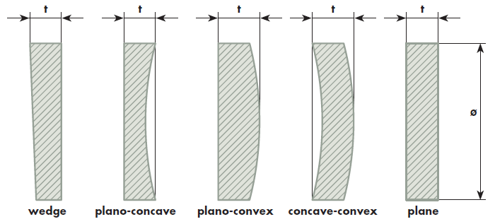
The shape must be specified for both sides separately. Basically, all combinations of plane, convex and concave surfaces are possible. A special role plays the wedge. A wedge (e.g. 30ʹ) can be applied on every kind of surface (plane as well as convex or concave). For curved substrates there are different conventions for the sign of the radius. Sometimes “+” means convex and “–” means concave. Other users refer “+” and “–” to the light propagation. In this case “+” means “curvature with the direction of propagation”, “–” means “curvature against the direction of propagation”. To avoid confusion please specify concave or convex in words or by the acronyms CC or CX, respectively.

The main decision should be the edge length or diameter. Unless stated otherwise the thickness description means the maximum thickness of the substrate, i.e. the centre thickness for plano-convex substrates and the edge thickness for plano-concave substrates. Consequently, a wedged plate is measured on the thicker side.
In order to achieve a good form tolerance one should take care for the ratio of diameter and thickness. As a rule of thumb the thickness should be the fifth part of the diameter. Of course, other ratios are possible but the production expenditure increases.

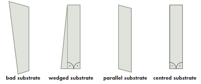
Beside size and material the tolerances are most important for the price. Of course, the optics must fit into the mount, so that the diameter should not be larger than specified. The most common specification is -0.1mm. Mostly, the thickness is free in both directions. LAYERTEC usually specifies it with a tolerance of ±0.1mm. There is a lot of confusion about the specification of wedge, parallelism and centring. Please note that wedge and parallelism describe the angle between the optical surfaces while centring describes the angle between the optical surfaces and the side surfaces (see figure 2).
LAYERTEC standard substrates have a parallelism better than 5arcmin. Specially made parallels may have a parallelism as low as 10ʺ. Standard wedged substrates have wedges of 0.5° or 1°. Larger wedge angles are possible depending on the substrate size. Normally, the 90° angle to the side surface has a precision of 20ʹ. Centring is an additional optics processing which improves this accuracy to a few arcmin.
Using the same nomenclature one can describe curved substrates. There should be distinguished between mirrors and lenses. The side surfaces of mirror substrates are just parallel. Nevertheless the direction of the optical axis can be inclined to the side surfaces. After centring the side surfaces are parallel to the optical axis. That way the mirror substrate becomes a lens.

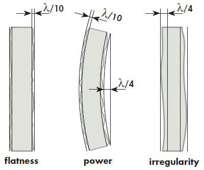
The surface form tolerance is normally measured by interferometers and is specified in terms of lambda, which is the reference wavelength. Without further statements the reference wavelength is λ = 546nm. To avoid confusion, one must clearly distinguish between flatness, power and irregularity. In the following, flatness and irregularity shall be explained for a plane surface.
Generally speaking, every real surface is more or less curved. Imagine that the “peaks” and “valleys” of a real surface are covered by parallel planes (see figure 3). The distance between these planes is called the flatness. This flatness consists of two contributions. The first contribution is a spherical bent of the surface, which may be described by two best fitted spheres for the “peaks” and “valleys”. The sagitta of this curvature with respect to an ideal plane is denoted as power. This spherical bent does not affect the quality of the reflected beam. It just causes a finite focal length. The second contribution is the deviation of the best fitted spheres, which is denoted as irregularity. This is the most important value for the quality of the beam.
The standard ISO 10110 provides a sufficient opportunity for specifying the surface form tolerance. Having the best comparability with the measurement results all values are given as numbers of interference fringes. They should be read as 1 fringe = λ/2. In the drawings the surface form tolerance is allocated as item number three: 3/power (irregularity)
Example: A slightly bent (λ/4) optics which is regular (λ/10) would be specified as follows: 3/0.5 (0.2)
Using the optics only for transmission (e.g. laser windows) the power as well as the irregularity do not matter. If the optics has the same thickness all over the free aperture the transmitted beam is not affected. The deviation from this equality is defined in a similar way as the flatness. It is also measured in parts of the reference wavelength and called “transmitted wavefront”. For instance, the window in figure 3 has a flatness of λ/4 but a transmitted wavefront of λ/10.”
Often thin substrates cannot withstand the coating stress. The coating will cause a spherical deformation. This means that a finite sagitta or power occurs. In case of circular substrates the irregularity is not affected by this issue. Taking the mentioned values seriously the flatness becomes poor. Nevertheless the quality of the beam is not affected.
MIL-O-13830 and ISO10110 are different standards for the description of optical elements. This often causes obscurities. Basically one should distinguish between scratches and digs. The scratch and dig numbers in MIL-O-13830 mean the maximum scratch width in tenths of a micron and the maximum dig diameter in hundredths of a millimetre. Maximum size digs can be one per 20mm of diameter. According to ISO10110 the defects are specified as item number 5. The grade number means the side length in millimetres of a quadratic area which is equivalent to the total fault area. So 5/1x0.025 means a surface fault area of 0.000625 mm2. Additionally, scratches of any length are stated by a leading L. A long scratch with a width of 4 microns would be specified as
L 1 x 0.004.
